Hi Guys, I have a question for any experienced 74xxx era chip hardware guy out there. It’s a bit complicated, so bear with me as I explain..
I have a working 80386 S100 CPU board which with a CPU input clock (CLK2 as Intel calls it) of 20 MHz. The bus itself and all support chips run at half this speed (10 MHz), Intel’s terminology CLK.
Works fine and can access up to 16MG RAM on the S100 bus with our 4MG RAM boards.
Andrew and I are adding “Daughter boards”, initially static RAM but later DRAM to get capacity (hopefully) into the GB range. For this I am using an “over the top” set of ribbon cables with connectors to join one (or more) boards to the CPU board which has all the address lines, data lines and a few control lines. Currently this arrangement is working nicely with a 2MG static prototype board. All this was challenging but alas now seems to be fine. 32 Bit access is working great (as is pipelining if you know what that is).
Here is my problem. The CPU is accessing that Daughter board at 10MHz but should be capable of running at a the max speed of the CPU, for my chips 40MHz.
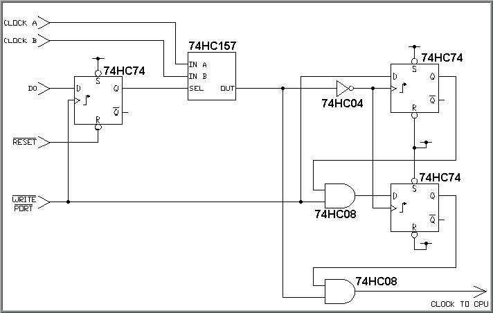
The obvious solution is to switch speeds (with 77LS682 address line logic) if a RAM access is above 16MG. Have that working fine too. But here is the problem, if I use a 2 line to one line output chip like a 74LS157 I glitch the clock more or less randomly.
Does anybody have a circuit where you can switch frequencies but guarantee that the instance of the switchover will not have one pulse (square wave) shorter that the shortest wave of the two frequencies. It probably does not matter if it’s longer but the CPU just does not seem able to take even one higher frequency pulse (because the switch took place between pulses). Hopefully I’m making myself clear. If not please let me know I will try and elaborate.
Any suggestions would be appreciated.
John
Attachment:
SwitchClockSource.gif
Description: GIF image