Increasing the FPGA ROM to 16K.
Up until now we have been running the Z80 monitor within a 4 K boundary from
F000H
to
FFFFH
with two 4K pages either of which can be switched in or out. This has
allow us to have a fairly extensive basic Z80 monitor and a separate menu
driven 4K section to access the IDE/CF card interface. It would be nice to
have a similar menu for the SD card interface. There is not
enough room in 8K to fit all this. The solution is to increase the
FPGA ROM module to 16K and have up to four 4K pages. The paging
process is exactly the same as for the 2 page 8K ROM except now we adjust
the address lines A12 and A13. At the moment I'm only using three 4K
pages:-
Page #0 A12 Low, A13 Low Output to Port
07H 00H Contains basic Z80 Monitor
SBC_MONA.Z80
Page #1 A12 High, A13 Low Output to Port 07H
01H Contains IDE menu and routines
SBC_MONB.Z80
Page #3 A12 Low, A13 High Output to Port 07H
04H Contains SD Card menu and routines.
SBC_MONC.Z80
Remember the only link between the 4K pages is the jumps at the start of
each module. You cannot call one routine from one section to another.
The changes within the FPGA code is trivial. We just change the 8K ROM
in the "ROM & RAM Interface" to a 16K ROM. We add in one more address
line (A13).
The trick however is building and loading up the
.HEX
file for Quartus.
As before we load up the Wellon
Programmer IDE. This time we place the 4K modules at
0000H, 1000H
and
2000H.
Hopefully these pictures are enough to explain the process.
Remember to point the Quartus ROM dialog box (when asked) to the correct
location of the
SBC-MON2_4+4K+4K.HEX
file. If you don't alter the file you don't have to reload the .HEX
file each time before a Quartus compile. The
SBC-MON2_4+4K+4K.HEX
is available at the bottom of this page.
The relevant Quartus .bdf file "upgrade" is
Z80_FPGA17.bdf. See the .zip file below
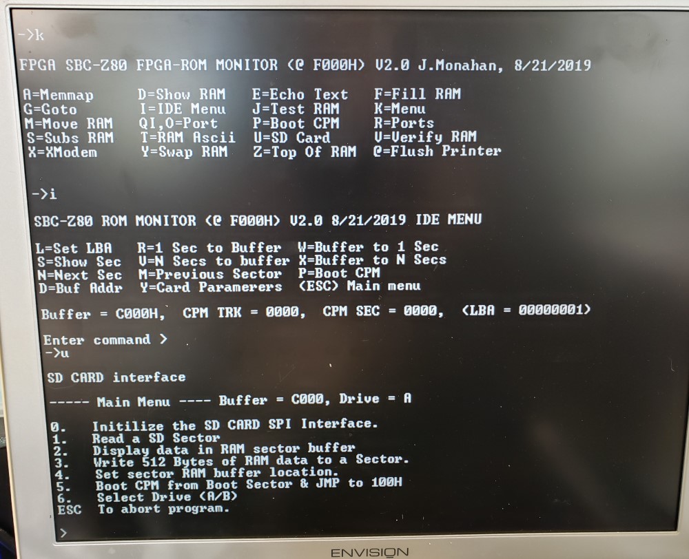
Here is a picture of the Z80 monitor with the 3 menus.
With 16K there is ample room to improve the above Z80
monitor!
SBC-MON2_16K.Zip
(This .zip file contains the Z80 monitor and FPGA .HEX files)
(V1.1 9/4/2019)
SBC-MON2_4+4K+4K.HEX
(This .HEX file contains the file for the 16K Quartus ROM)
(V1.1 9/4/2019)
Z80_FPGA17 -- (16K Rom Added)
(V1.1 9/7/2019)
More additions later!
Other pages describing my S-100
hardware and software.
Please click
here
to continue...
This page was last modified
on 05/20/2020