S-100 Bus 12 Slot Motherboard
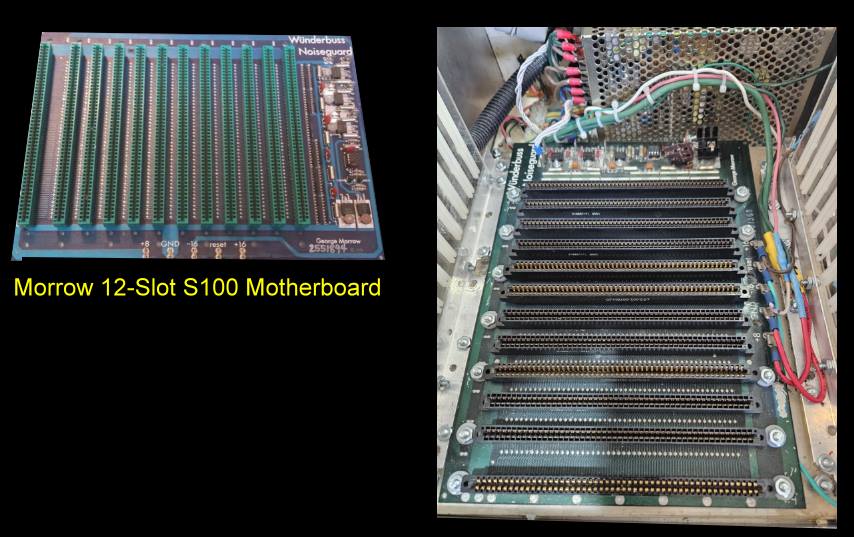
My current "Test S100 bus
System" is now over 15 years old. Countless S100 boards have been pulled in
and out of the system. The front S100 bus connector has been replaced two
times. It is a George Morrow 12 slot "Wunderbus" Motherboard. Here is a
picture of the setup:-
The board has on-board active termination and excellent ground plains to
yield clean reliable S100 bus signals. Unfortunately it is not a
common motherboard and rarely appears on eBay.
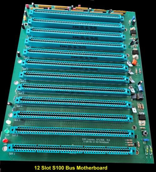
I decided to construct and build my own. This turned out to be
more difficult (and expensive) than I expected. It took 4 prototypes to get
everything right. Early two layer designs done with KiCAD were just
not reliable at high speeds. Four layer boards with two internal ground
planes were better but failed with chips using 74VLCxxx bus buffers such as
those used in our FPGA
Z80 CPU board.
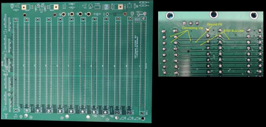
In the end I had to hand layout a four layer board with two internal ground
planes and ground flood planes between the S100 bus traces on the top and
bottom of the board as well as between the S100 bus connector pins. I
could not get KiCAD (V4.1) to do this! It took a full day of work.
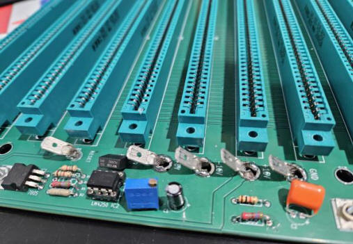
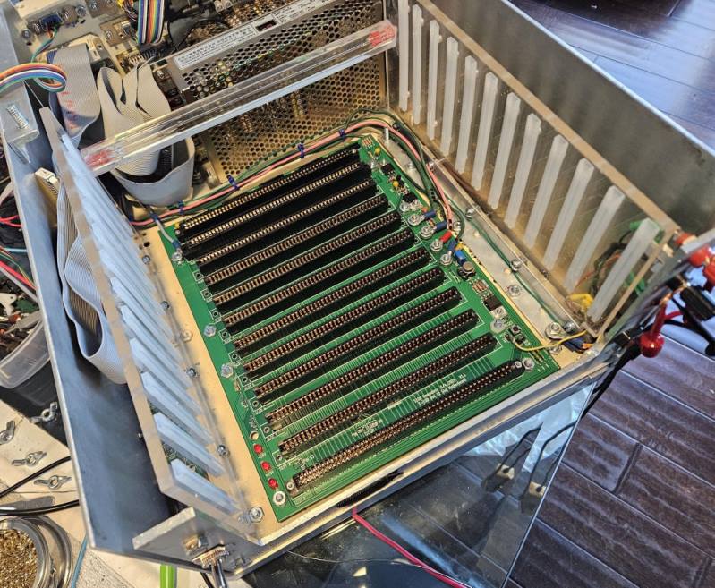
Here is how the final board looks:-
The trick is to place small vias between the traces that connect to the
inner two layer flood ground planes and let KiCAD then do a ground fill in
the local area
Active Termination
Active termination of a bus is where we prevent buss signals running down
the bus and bouncing back from the end creating noise on the bus. A number
of approaches have bee used. For simple TTL logic the most effective way is
to mention the bus line when not drive low or high at about 2.3v-2.6V.
Easily done with a pull-up and pull down resistor. However for 100 bus lines
this is inefficient power wise and largely unchangeable.
A better solution is to use an adjustable OpAmp circuit to set the line
voltage. Here is the circuit we will use:-
| |
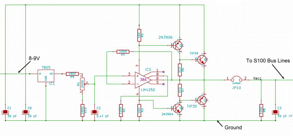 |
By adjusting R1 which alters the input to the LM4250 OpAmp you can set the
bus line between ~2.0V and ~3.5V. Every (non-power) S100 bus line has
a 1K pullup resistor.
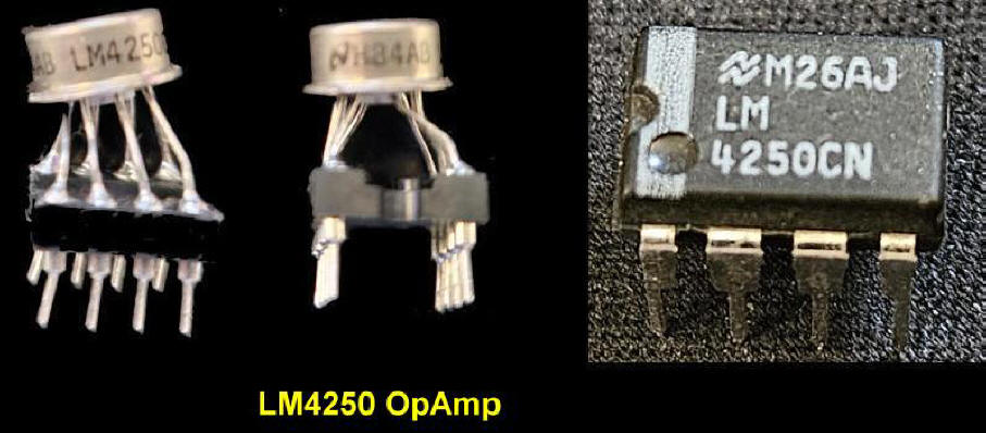
The LM4250 is meant to be an 8 pin dip. This is
now a fairly old/rare part. I got mine on eBay. The "CAN" versions are more
common.
You can bend the pins into two rows of 4 and solder the unit into the socket
IC2. Then solder the socket into the board as shown here:-
Examine the datasheet to identify pin1 from the
LM4250 datasheet. It's important this unit is not too high or it
will interfere with the S100 board above it.
Building The Board
This board has over 1200 solder joints so set aside a good block of time to
do it carefully. It took me a full day to do this board. Most components are
straight forward and common. Please study the schematic before building the
board. Install all the components on the board. The
TIP29 and TIP30
transistors do not need heat sinks. Make sure you solder in the 1K OHM
resistor packs in the correct orientation. I like to use 10 pin linear
sockets for these in case you need to change the value of the resistor SIP.
Add the three LEDs D1,D2
and
D3 with the long lead in the square pads.
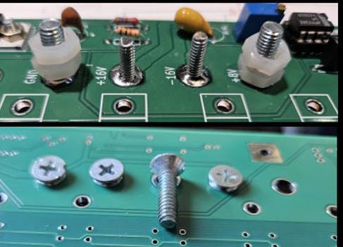
The four power connections are screws as shown here:-
These are standard wire clip connectors.
You can use screws if you like as shown above, however be very careful the
metal of the screws does not touch the back and front of the board. Make
sure the bolt heads at the back just cover the pads. This requires flat
angled head bolts as shown above. Because these pads carry a significant
current (particularly the 8V line), they should be soldered into place as
shown above.
On the top side to be safe I add a plastic washer before adding the
connecting wire and nut.
Before adding the S100 bus connectors temporally hook 8 volts to the +8V
nut. Carefully adjust the 2000 Ohm Pot R1 so pin 1 of
JP10 is
2.3V.
Then install all the jumpers on the board,
JP10 included. Check each pin is 2.3V
(except 20, 53
70, 1, 51, 2, 52, 50 and 100).
The S100 connectors are expensive so it is
necessary to allot a good block of time to solder them in correctly.
The pads are very close on this board so be careful to use as little solder
as possible. The ground pins need more time to heat the pads on this board,
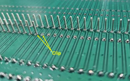
The connectors I used (see below), had extra long solder pins which
protruded on the bottom of the board. I carefully clipped each pin down to
the solder joint.
Here is a picture:-
Just to be safe I like to test the whole board with just 3 connectors first,
(Slots 1,6 & 12). Hookup the power again and check all connector pins for
2.3V.
To test the board I use the
Propeller Board, the
4MG RAM board and the
Z80 Master CPU board. The Z80 monitor must boot every time.
The three power LEDs should light up.
If all is OK, add in the remaining connectors. When done, again check for
2.3V on the S100
bus connector pins.
Computer Box Assembly
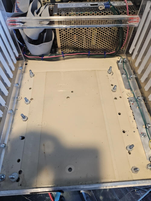
Next we need to prepare the board support. Its critical none of the bottom
protruding S100 bus pins touch the floor of the computers case. To be
safe I have a layer of clear plastic film on the floor of the box case.
The board is supported with 9 mounting bolts. Each bolt has a thick plastic
nut/washer so the whole motherboard is raised away from the case floor.
Carefully insert support screws as shown below. Each screw is tightened
into place with a nut and on top is placed a plastic washer. This insures
no traces on the board contact the screws/case.
See below.
Next insert the motherboard in the case and tighten it down. Hookup the
four power supply lines and again check some lines for
2.6V.
If you are using an external push button reset switch (besides with SW1) you
need to hookup one of the switch's two wires to P12 pin 1. The other
switch wire goes to ground.
Pressing this external switch should zero the
S100 bus line 75.
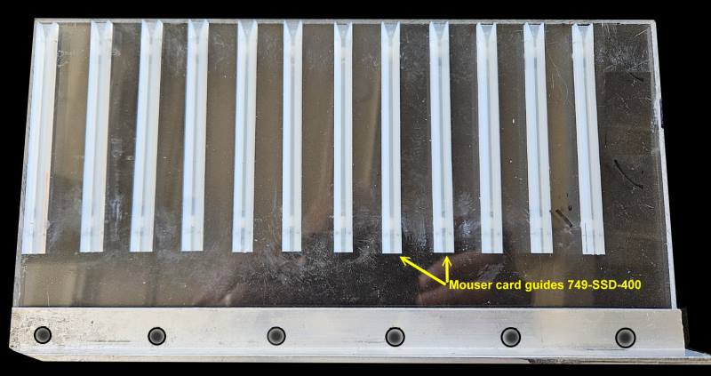
All that now needs to be done is add the card guides. There are various
ways you can do this depending on your case configuration.
I have used two Plexiglas supports with holes to accommodate each card
guide. It's tricky to get the card guide drill holes right. It took me
three try's!
The height of the card guide has to be the exact height of an S100 bus card
in a slot. This way board card ejectors work correctly.
For testing use as few boards as possible. I started with
The
Propeller Console IO Board, the
4MB RAM board and the
Z80 CPU board.
All my
"regular" S100 boards work fine with this motherboard. However I found that
in order to run it with boards that utilize
74LVCxxx
buffers (such as the FPGA
Z80 CPU board) it was necessary to replace the 270 Ohm network resistors
pulling up each S100 bus line in the classical Compupro motherboards with a 1K resistor network.
This appears to be due to the differences in the current sinking differences
between
74LSxxx
and
784LVCxxx
chips.
PARTS
Getting 100 pin connectors is a challenge these days. I got mine from eBay.
You can do a web search for 100 pin edge connectors.
Newark has them at $17 each! (Part
Number 85H7582)
.
The card guides also are tricky to find. I use Mouser ones. (Part Number
749-SSD-400).
I got the
LM4250
from Quest Components. It was the CAN type. I got an 8 pin DIP version from
eBay.
A
TIP29C or TIP32C NPN
transistor can be used instead of the older
TIP29
A
TIP30C or TIP32C PNP
transistor can be used instead of the older
TIP30,
transistor
All there other components are fairly common.
Notes.
This motherboard uses the IEEE-696 specs for the S100 bus (S100 bus pins 20,
70 and 53 are grounded). For older per-IEEE-696 boards jumpers P16, P17 and
P18 should be removed.
Please note this is a completely custom board. While the board mounting
holes correspond approximately to the positions in a
Compupro box it is best to consider a completely customized S100 system
with this board.
Also read
here
for a description of a similar 9 slot motherboard and
here for an advanced
S100 bus system by Jeffrey Wilson.
Note that often S100 motherboards and boxes appear on eBay at very reasonable
prices. These motherboards have "no moving parts" and are often a
quicker/simpler solution to building an initial S100 bus system.
A good place to look is
here.
To Order a Production S-100 Board
Realizing that a number of people might want to utilize a
board like this together with a group of
people on the
Google
Groups S100Computers Forum, a "group purchases" is now
closed.
The links below will contain the most recent schematic
of this board.
Note, it may change over time and some IC part or pin numbers may not
correlate exactly with the text in the article above.
MOST CURRENT MOTHERBOARD SCHEMATIC
(for the 12 slot board) (V6.1B 9/3/2021)
Most current KiCAD files for this motherboard
(for the 12
slot board) (6.1B 9/3/2021)
Most current Gurber files for this motherboard (for the
12
slot board) (6.1B 9/3/2021)
This page was last modified
on 09/03/2026