
| Home | S-100 Boards | History | New Boards | Software | Boards For Sale |
| Forum | Other Web Sites | News | Index |
 |
|
 |
 |
 |
 |
 |
 |
 |
 |
 |
 |
 |
 |
 |
 |
 |
 |
 |
||
 |
 |
||
 |
|||
 |
 |
 |
 |
 |
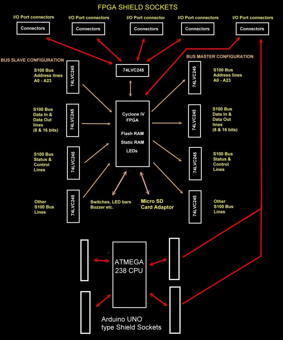
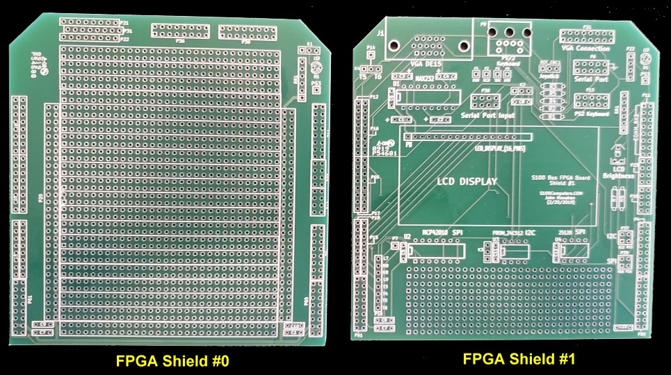
| Board Circuit Name (Click to Select) | FPGA Shield Board | Board Description | |
| UART_PORT_V2 | #1 | A simple UART port interface to the S100 Bus. | |
| 1602 LCD Display_V2 | #1 | Interfacing to a dual line 1602 LCD Display Module | |
| A VGA PONG GAME_V2 | #1 | A simple VGA interface demo. | |
| RAM_DEMO V2 | #1 | A 4K OnChip Static RAM Circuit | |
| PS2_KEY_V2 | #1 | A simple PS2 keyboard input port example | |
| PS2_LCD V2 | #1 | Display a PS2 keyboard input on a 1602 LCD Display | |
| SPI INTERFACE V2 | #1 | An SPI 16 bit Communications Interface to a Digital Potentiometer | |
| I2C INTERFACE_V2 | #1 | An I2C Communications Interface to an EEPROM | |
| SPI_INTERFACE V2 | #1 | An improved SPI interface with 8, 16, 24, 32, .... bits | |
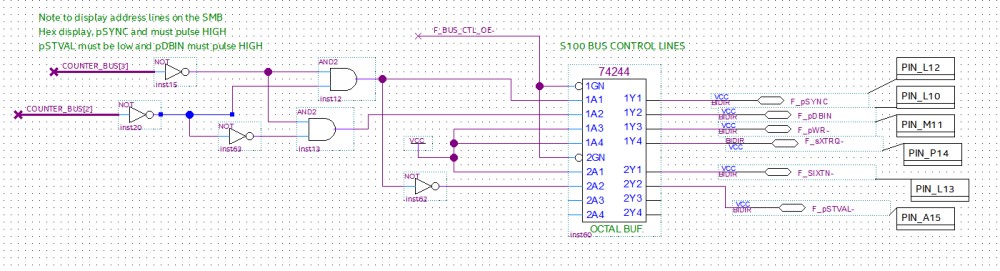
| VGA CHARACTER DISPLAY | #1 | A VGA Terminal Character display within the FPGA |
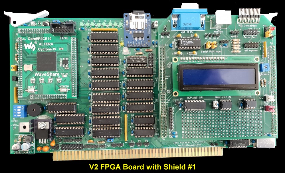
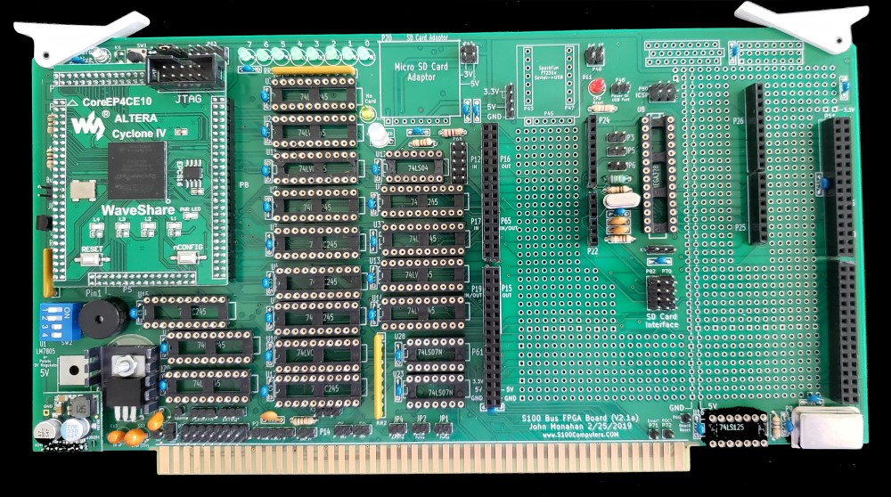
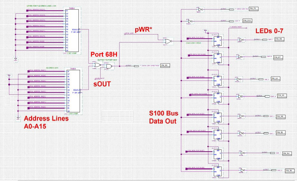
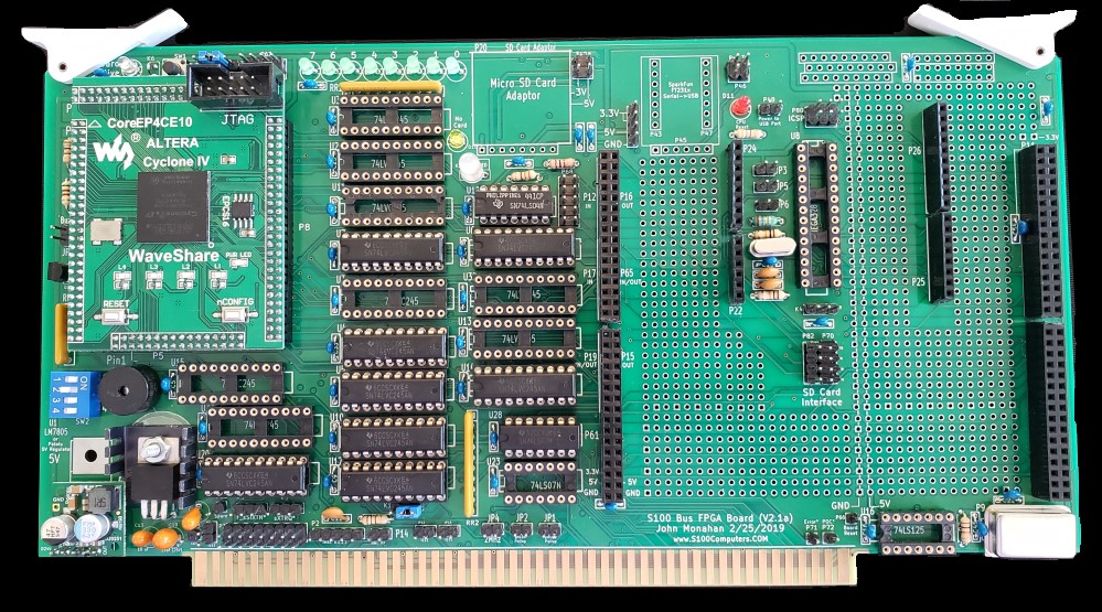
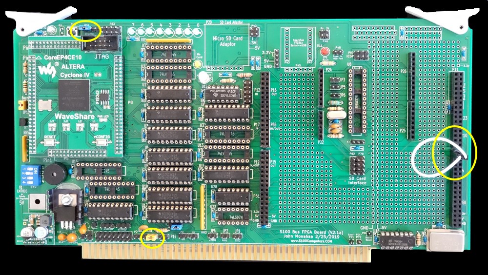
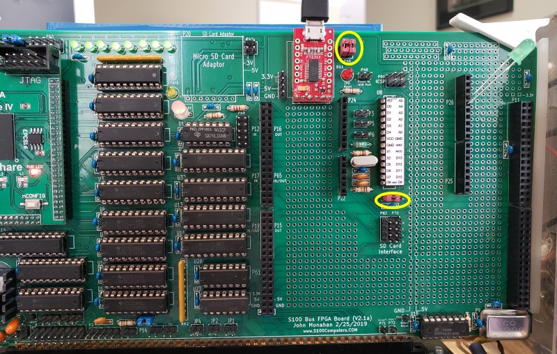
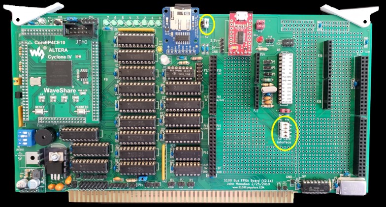
There appears to be a few variations of the 74LVC245 20 pin DIP level Shifters chips with "A", "AN" etc after the 245. As best I can tell so long as they are 20 pin DIPs they are all OK. I use Mouser chips # 595-SN74LVC245AN. The WaveShare Cyclone IV adaptor can be obtained directly from Waveshare. The WaveShare unit uses unusual 2mm dual row pin connectors. Unlike to normal 0.1" connectors these are quite rare an expensive (Digi-Key #S5750-30-ND). You need to carefully cut them to size, carefully cutting off the extra pins with a wire cutter. The USB serial Adaptor is from Sparkfun F1231x. The Micro SD Card adaptor is from AdaFruit.
 |
This page was last modified on 08/06/2024