An S-100 Bus
FPGA Video & LCD VGA Display Board.
Introduction
Many S-100 board manufactures had their own Video boards. Most initially were character based "video TTY's". The very early ones were restricted to 64 characters/line (for example the SSM board), but soon 80 characters per line became common. A good example is the SD Systems 8024 Board.
As time went on, boards started to get more sophisticated and began to offer fairly high resolution graphics capabilities. A good example of this would be the
Matrox ALT512 board which offered color graphics at a 512 X 256 resolution. There were even a few of higher resolution. The NEC 7220 based video controller boards for example, which brought video display graphics to a new level. That chip was the NVIDEA chip of its day back in the early 1980's.
Once the IBM PC appeared on the scene video hardware compatibility with it became key. There were a few S-100 bus attempts to make equivalent cards. The Lomas "Color Magic" IBM-PC Color Graphics Adaptor (CGA) look-alike probably being the most successful. However with the phasing out of the S-100 bus in the late 1980's, no higher resolution S-100 video boards were ever produced.
Here is a Cyclone IV driven VGA text compatible S100 bus board. Please not this
is not like our
Trident chip driven VGA Board where true IBM PC VGA color graphics can be
displayed. It is primarily a text display board with 8 different colors.
It is however fast with 80X38 characters/line. Unlike the Triton
chip driven VGA Board however this board can be used with a Z80/CPM setup.
It can in fact replace our
Propeller Driven
Console IO Board
Also on this board is a small LCD display that is completely independent of the
VGA display. It can be used to display supplemental computer information.
It has the following capabilities.
1. A 50mHz FPGA Z80 driven CPU to
display text sent to an S100 Bus parallel port.
2. This port block can be anywhere in the Z80's address space using an
onboard 8 position dip switch. The default block is 80H-8FH
3 If this port is set to 00H-0FH the board can act as a
direct replacement to our
Propeller Driven
Console IO Board . In this arrangement keyboard input is via a
PS2 keyboard port on the board.
4. With an 8088 or 80486 CPU the board acts as a VGA
text board at A000:0000H.
5. The board has IBM Compatible X,Y cursor/text positioning
(just like our
Propeller Driven
Console IO Board , the
Lava VGA board and
Trident SVGA Board).
6. The board has a separate completely independent onboard
OLED for text sent to one of the boards ports.
7. There is an IBM PC compatible parallel printer port
8. All ASCII characters sent to the board also show on an
onboard LED Bar as well as two status bits.
9. The board has an IBM PS/2 keyboard port and onboard buzzer.
10. There is an onboard 4 pin configuration switch for various
options.
What Is Needed
The FPGA we will use here is an
Altera/Intel
Cyclone IV FPGA. This chip is currently in about the middle range
of the programming capacity of FPGA's. The actual chip uses a
"Ball Grid Array" method of soldering it to a printed circuit board.
This requires some specialized equipment, so normally one purchases an
"adaptor board" for these chips with the chip on it. Besides providing "normal" pin
attachments to (in our case), the main S100 board, these
adaptors contain a number of voltage regulators, Flash RAM, a programming
socket and other components these FPGAs require to operate.
As for our previous boards we will use the WaveShare "CoreE4CE10"
Cyclone IV board adaptor, (however for this board we only need the two side
rows of pins). Its schematic can be seen
here.
The second thing you will need is a device to program the FPGA chip itself.
There are many FPGA programmers available. I really like the
USB Blaster (V2)
that Waveshare sells. Its simple and reliable. And importantly, works
directly within Intel's Quartus V12 (see below).
Somewhat unexpectedly you will need to pay particular attention to the
special very tightly spaced pins on the above adaptor board. Because
there are so many FPGA output pins, its not practical to have a connector
with the standard PC board 0.1" pin spacing. The above WaveShare unit
uses unusual 2 mm dual row pin connectors. Unlike to normal 0.1"
connectors these are quite rare an expensive. If you solder these female
sockets to the board the WaveShare adaptor sits quite high on the board and
will prevent the next S100 bus slot from being used. If you carefully
remove the JTAG socket top border edge with a wire cutter - all around about
1/8", it will fit into most S100 bus motherboards without taking up two
slots. Alternatively you can solder the adaptor directly to the S100 board.
Of course removing the adaptor is all but impossible in this case.
Please note the 2 mm dual row pin connectors (Digi-Key #1212-30-ND sockets)
for the WaveShare adaptor are quite tricky to fit on to the board. I
found the best way to do this (after trimming them to pin size), is to push them half way
on to the adaptor pins and then wiggle them to fit the whole unit on to the
S100 board. Figure on spending 10 minutes on this step!
Do not solder them to the board first and then try and press the adaptor
down on them. They are very fragile and internally the leaves will
bend if socket angles are not exactly correct. When in place, check
each pin is visible on the back of the board before soldering. Only
then solder all around. Add as little solder to each pin as possible -
the narrow pins have a tendency to wick up solder internally. I find
it best to have the socket base slightly above the front board surface when
soldering in the first two pins. Wedge a sheet of thick paper between the
socket and the board initially. Better
sockets are the Mouser #437-8338703810001101
38 pin sockets (carefully
clipped to size). However these sockets are often out of stock at Mouser
The LCD display is driven by either an Adafruit
ESP32 Tiny S3 or a
Waveshare ESP32 S3 Zero.
Currently I'm recomending you to
use the ESP32 S3 Zero.
The code for the ESP32 TinyS3 is not complete yet.
The 1.54 Inch OLED Module 12864 128x64
SSD1309 LCD Display is available from a number of
suppliers. I got mine from Amazon.
The TinyS3 unit goes in
P5+P6 sockets. The
S3 Zero goes in
P17+P18 sockets.
There seems to be a two types where the four connecting pins are
GND,VCC,SCL,SDA
and VCC,GND,SCL,SDA. There is a jumper on the board (P25) to
accommodate
the power for both types.
Check the voltage on pins P1 and P2 and jumper P25 to match. Only then add
the OLED unit.
Note there are also other similar size OLED displays that have more pins and are
not I2C driven. The above ESP32s assumes an
I2C interface.
The rest of the boards components are standard -- available from Jameco,
Mouser, Digi-Key etc. For prototype boards I generally use "double swipe" IC
sockets.
For a critical board like this I prefer to use "Machine Tooled" IC
sockets. However they are more expensive and you have to be particularly
careful not to bend the actual IC pins.
Quartus Prime.
For Altera/Intel FPGA's the program of choice to program them is called
Quartus Prime. This a very large Windows based IDE
interface. It is completely self contained with everything you need
to write FPGA code and program the chips. Its an expensive software package.
Fortunately Intel supplies a "Quartus Lite" free version
for students and people like us. Even this is way overkill for our use. The
most recent version can be downloaded from
this Intel site. The package will take ~20 minutes to
install on Windows 10. You may want to first review
this
video about the installing process. Please see the Notes section at the
bottom of this page for more help installing Quartus.
Please keep in mind that programming an FPGA is different from the normal
linear/sequential programming approach you may be used to. On an FPGA
everything is potentially happening at once. Good FPGA programmers
take years to excel and currently are in high demand. Timing
and power distributions across the chip almost become an art form.
Fortunately out needs will be far simpler. Also there seems to
be an excellent community of experienced people ready to help -- beginners.
I have found the
Intel FPGA Forum to be very useful and helpful. However by far
the best way to get started is to look at a few YouTube demonstrations.
One outstanding YouTube video to get you going with Block Design File FPGA
programming is this one by
ClockFabrick Electronics Academy.
Note, click on the "full screen icon" for easy viewing. Use ESC to return.
Also
please allow a few minutes for it to download. It's a very large (50 minutes)
video file.
For absolute FPGA beginners, rest assured, you can more or less use the FPGA
code examples below as "Black boxes" to get this board up and running. However
you will be missing one major aspect of the board. By stepping along and
understanding how the FPGA code works you will in the end have the ability to
modify the board in amazing ways.
Board Construction
There is nothing particular special about constructing this board. Use
the normal construction process we have in the past. Be careful with LED
orientations. The longer lead goes into the square hole.
Check also the orientation of resistor networks.
There are two sockets for the Pololu 5V
and 3.3V regulators. While the older ones
(D24V25F5) are still available
and use P1, it seems Pololu is suggesting users use the newer
D24V22F5's
(5V, 2.5 Amp) units, it has a different pinout, use this one in P57. More
recently they also added the equivalent
D24V22F3
3.3V regulators. Use socket pins P11. If you use the older Pololu
D24V25F3
3.3 V regulator use socket P4. Note, you can also use the (less
expensive) EzSBC
regulators in P67 and P11 (the rightmost 3 pins in each case).
Solder in all the IC sockets, caps, resistors, video filters, etc. Note
C23,C18,C8,C33,C32 and C29
are
47pF caps. The
other caps on the board are
0.1uF (except the
voltage regulator caps 30uF and 10uF). Solder in the buzzer with the "+" side on
its RHS. I generally solder in dip switches directly to the board.
For the 10 LED Bar display I like to use a DIP socket. It's easy to get the
display in the wrong way. Its pin 1 should be on the bottom LHS. The PS2
keyboard socket needs to be modified. Clip off the 3 outer shielding legs.
Space the 6 pins to fit into the P2 holes. After soldering in the pins put a dab
of solder on both sides of the socket case to the board's ground pins.
Add the 4 LED's. The colors are up to you. The long lead to the square pad. I always use blue for the "Board
Active" LED. Do NOT solder in the dual LED at K2 yet.
Without any chips on the board pop the board into the S100 bus and check you are
getting 5V or 3.3V going to each IC socket.
If this is OK install all IC's to the board, including the
ESP32 TinyS3 (in
socket
P5+P6) or
ESPS3 Zero
(in socket
P17+P18).
You will note that if you set the switch SW3 to
00H the console IO ports
will be the same as the
Propeller Drive
Console IO Board. We will explore this later.
For testing we will leave our Propeller Console IO board in place and set SW3 set to 80H-8FH
as shown below.
Both the Z80 CPU "Master Monitor", the 8086 and 80386 monitor code have been
updated to accommodate this board. More on this later.
For now set the SW1 "configuration" dip switch as shown here:-
Z80 Port 86H should read 00000111B. This tells the S100 Bus Z80
monitor the board is available.
VGA output can be from the P9 15 pin VGA connector or via a ribbon cable from
2X8 pin connector as we used for all VGA connections with our boards (i.e. same
pinouts).
Jumper P23 (Phantom), K1 2-3. JP7 (Buzzer), P24 (USB power). Do not jumper
P21 or P22, P26 or P27.
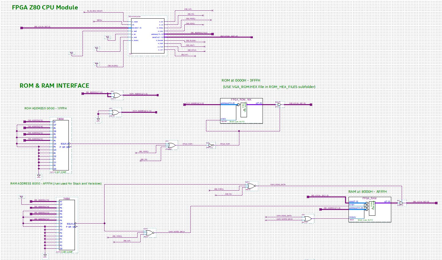
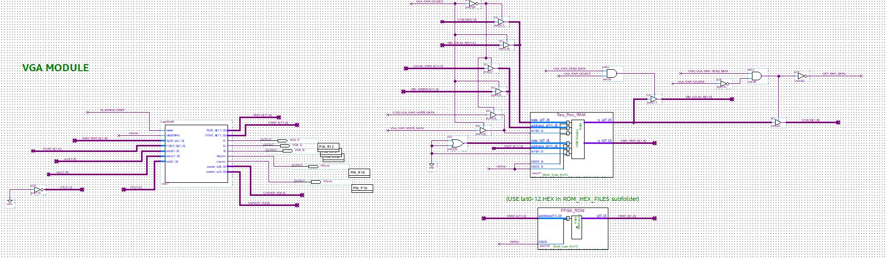
The FPGA VGA Z80 Code
The FPGA code for this board is not
extremely complex but interfacing it with S100 bus software as we will see is
tricky.
As far as possible everything is done within the FPGA and its ROM/RAMs.
Simple IO calls from the S100 bus to display characters etc. is all that is
needed.
The .brd file code divided into 3 sections for the VGA display, the LCD display
and the Printer port. The FPGA has an internal Z80 CPU running at 50mHz to
handle everything.
Before we start, a few things about our FPGA code file directory structure.
You have to be very careful with Quartus where you place your files. The actual Quartus "Project file" work
Z80_FPGA.qpf should reside in the main folder you will build your programs. In my case it happens to have a path:-
C:\intelFPGA_lite\18.0\quartus\MyFPGAPrograms\Z80_FPGA_VGA\Z80_FPGA
The above path (in yellow) is the root below which we will build all files in this project. Your path may be different but the
Z80_FPGA_VGA directory must exist.
The actual
Z80_FPGA_VGA.bdf in this directory.
It s
the current "work file" which when compiled we use to program the FPGA.
The onboard FPGA Z80 requires a small ROM to handle some of the simple Z80 processes below.
The Z80 code file is FPGA_VGA_ROM.HEX.
Because it's at 0H
in RAM we don't have to relocate the code for Quartus to pick it up (as in the
case for example of the FPGA_Z80_SBC ROM).
All the required files are at the bottom of this page. Unless you modify
the FPGA code you don't have to alter anything. If you do modify
FPGA_VGA_ROM.Z80 with a Z80 assembler, you must let Quartus know where the
new FPGA_VGA_ROM.HEX file
is. I always put the new .HEX files in:-
C:\intelFPGA_lite\18.0\quartus\MyFPGAPrograms\Z80_FPGA_VGA\Z80_FPGA\HEX_FILES\
If you later do want to change the default board operation and need to change
the FPGA Z80 code, right click on the "FPGA_ROM_16K"
module within theZ80_FPGA_VGA.bdf
and select the IP parameter Editor
to let Quartus know where your new FPGA_VGA_ROM.HEX
file is.
The FPGA utilizes the VGA display we have used successfully on other boards (e.g..
the FPGA_Z80 SBC). It
came from the The
Open Cores Web site. This module is a Text Mode Monochrome Video Display
Adapter for VGA monitors.
It is about the same as the original IBM MDA card
appeared in 1981.
The FPGA Z80 handles all characters for the screen, updating the cursor etc.
The code is inFPGA_VGA_ROM.Z80.
There is a console status port and console data port just like our
Propeller Driven
Console IO board. The two ports are completely settable with the Dip
Switch SW3. The board utilizes a block of 16 ports which can start from
0H to 0FH. (if the
board is used instead of the Propeller Console Io board). The
default location however is 80H-8FH.
The FPGA Z80 also has a small ROM module (FPGA_RAM) at 8000H within the
FPGA. Its only use is for the Z80 stack.
Here are the boards ports:-
S100_CONSOLE_STATUS EQU 00H ;S100 Bus
Console (Propeller Console Board)
S100_CONSOL_STATUS EQU 00H
S100_CONSOL_OUT EQU 01H
S100_CONSOL_IN EQU 01H
VGA_CONSOL_STATUS EQU 80H
VGA_CONSOL_OUT EQU 81H ;Port to send data to VGA display
VGA_IOBYTE_PORT EQU 86H ;Port to communicate with VGA console IO
ACTIVATE_LCD_PORT EQU 88H ;This pin must be 1 for the ESP32 code to respond
PS2_CONSOL_STATUS EQU 89H
PS2_CONSOL_DATA EQU 8AH
PRINTER_STATUS EQU 8BH
PRINTER_DATA EQU 8CH
PRINTER_STROBE EQU 8DH
LCD_DATA_PORT EQU 8EH ;Port to send data to LCD display
ESP32_RESET_PIN EQU 8FH ;Reset the ESP32
In order to test this board I have written a short Z80 program (FPGA-VGA.Z80) to run at 100H in
RAM.
Load FPGA_Z80.COM
(see below), to RAM at 100H with the Master monitor
X command.
Then type G100,
you should see:-
Hook-up your VGA cable to the board. Either the ribbon cable connector
(P3) or the DB15 VGA socket (P9). (The pinout of P3 is the same as all our
previous boards with a VGA ribbon cable connector).
Take option 7. You should see each keyboard character typed on Propeller
Console IO board appear on the VGA screen.
You should also see the ASCII bit pattern displayed on the 10 LED Bar display.
You can change the text color with option 4.
The console IO code in the above demo program is just a few lines of Z80 code
and can be easily incorporated into any BIOS.
While far from complete, the Z80 code within the FPGA can handle many ASCII ESC
control characters completely transparent to the source.
You can add more by modifying FPGA_VGA_ROM.Z80.
Note no Z80 S100 bus RAM is utilized to display text with this board.
I.E. It's IO mapped nor memory mapped.
Now is a good time to insert the dual color LED at K2.
Insert the 3 pins
one way. Load and run the above program again. If the LED is green its in
the correct orientation. Solder it in place. If it is RED flip it around
so it is green.
This way
GREEN = Z80 Mode,
RED = 8088/8086 mode (see below).
Here is the relevant Z80 Section or the
Z80_FPGA_VGA.bdf file:-
The FPGA VGA 8088/80486 Code
To run the board with an 8088 or 80486 things get more complicated.
In order to be compatible with
MSDOS a video
RAM display area must be present. We will use the location
A000:0000H - A000:FFFFH
to be IBM PC compatible.
There is one further complication. We first came across this with our
Trident SVGA Board.
Because all our current 8086, 80286 or 80386 CPU boards cannot send 16 bit
data as two back to back 8 bit chunks (they send them as 16 bit data), the board
is not capable of working with these CPUs. The FPGA code could be modified
to handle back to back 8 bits but it is a lot of work. I chose to
concentrate on the 8088
(always 8 bits) or the 80486
which can send 16 bit data as two back to back 8 bits -- at least for now.
BTW the only S100 8086 CPU board I know of that actually does 8 bits back to back
is the
TecMar one. Unfortunately I don't have one of these to test. If
somebody has time the FPGA 80286 SBC could be modified.
In this mode the onboard FPGA Z80 is completely ignored. All ASCII characters
are placed directly in RAM starting at A000:0000H by the 8088/80486. The
LED bar is still active displaying the current ASCII character and status bit.
The K2 dual LED will be
RED
When MSDOS loads it always checks to be sure a "VGA ROM" is present at
C000:0000H. The first two bytes should be 55H,AAH to tell it an IBM PC
compatible video board is present. A software INT 10H with various
parameters control the board. (See below). In our case since we will use
00H,AAH to flag the MSDOS BIOS/ROM monitor that our FPGA_VAG board is present.
With both our 8086/8088 and 80386/80486 monitors the code has be significantly
updated to allow MSDOS to talk to 4 different video board.
Before launching MSDOS (with the "P" command) you must use the "B" command to
select the MSDOS video board in the
8086 Monitor
or
80386 Monitor :-
The four boards are::-
0 =
The Propeller Console IP Board
1 =
The Trident VGA board
2=
The Lava video board.
3=
This FPGA_VGA Board
If the B command is not used the default MSDOS video board will always be the
Propeller Console IO Board.
Note the above option utilizes the most recent monitor versions (8086
V10.7) and (80386 V1.9). These are available in links below.
In order to test this board I have written a
short A86 program (VGA_S100.A86) to run at
0000:0100H in
S100 bus RAM.
Load FPGA_S100.BIN
(see below), to RAM at 0000:0100H with the 8086 monitor
W
command.
BTW, you could also load it into RAM at 100H with the Z80 Master monitor with
the
X
command and then switch to the 8088/80486
with the "O" command.
You should see:-
All the menu commands should be fairly clear. Menu item 8 is to
check VGA ROM BIOS can handle cursor positioning.
Note
MSDOS (V4.01)
requires a keyboard interrupt to function.
Here is a picture of the FPGA_VGA Board booting MSDOS:-
Most MSDOS Programs just use character screen placement just after the last
character. However some MSDOS programs actually place each character
at a specific X,Y coordinate on the screen.
The second picture above shows the MSDOS program
FDISK.EXE doing this.
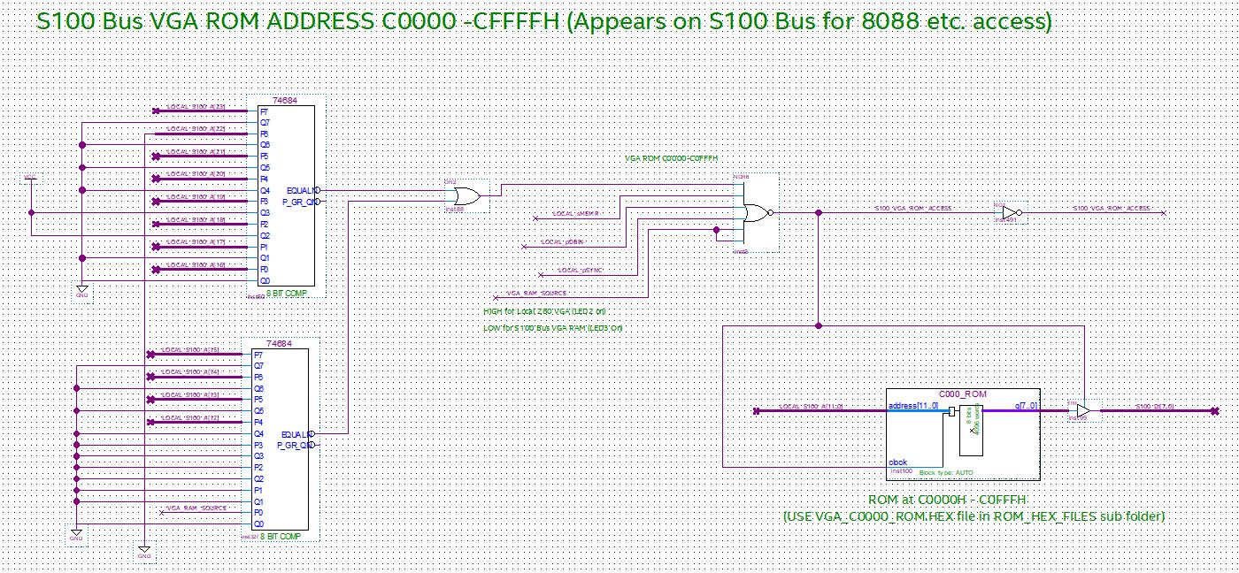
All of this is done by doing a monitor far call to the following jump table at
C000:0000H.
ORG 0H
;FPGA ROM CODE WILL LOAD AT C000:0000H
DB 00H,0AAH,'<--IBM_VGA_LCD Board ROM BIOS.'
DB ' (JMP table at C100H)'
TIMES 100H-($-$$) DB 0
;Jump table always begins at C100H
INITILIZE_VGA: JMP INIT_VGA
;C000:0100H, Text Color in CL
CHARACTER_OUT: JMP DO_CHARACTER_OUT
;C000:0103H Standard print character at current cursor position
SET_CURSOR_X: JMP MOVE_CURSOR_X
;C000:0106H Move Cursor X posuition (value in CL, 1...79,0)
SET_CURSOR_Y: JMP MOVE_CURSOR_Y
;C000:0109H Move Cursor Y position (value in CL, 0-27H)
SET_COLOR: JMP CURSOR_COLOR
;C000:010CH Change screen character color (31H-37H)
GET_CURSOR_X: JMP ASSAY_CURSOR_X
;C000:010FH Get Cursor X position
GET_CURSOR_Y: JMP ASSAY_CURSOR_Y
;C000:0112H Get cursor Y position
GET_COLOR: JMP ASSAY_CURSOR_COLOR
;C000:0115H Get character color
For example for a MSDOS program to print a character at the next character
position we would have:-
DO_VGA_KEYBOARD:
CALL ZCI
;Routine to input from Propeller/S100 bus keyboard, send to VGA
MOV CL,AL
CALL word
0C000H:CHARACTER_OUT ;Go to FPGA ROM with
character in CL
RET
The code is simple and fast. The actual character processing/placement is
all done in the FPGA ROM visible to an 8088/80486 at C000:0000H.
Most people will not need to modify this Quartus .brd file ROM.
The source code for this ROM
VGA_C000_ROM.A86
is provided at the bottom of this page.
Unlike the
FPGA Z80 ROM
above this code must exist as a .HEX file starting at
C000:0000H.
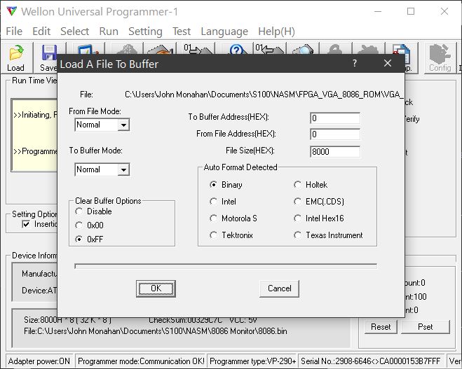
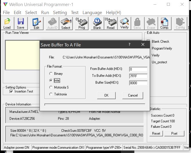
I
cannot seem to get the NASM assembler to generate .HEX files. I use the
trick of using the Wellon Prom burner software to convert a .bin file to a .hex
file.
Remember the final .hex must reside at:-
C:\intelFPGA_lite\18.0\quartus\MyFPGAPrograms\Z80_FPGA_VGA\Z80_FPGA\HEX_FILES\VGA_C000_ROM.HEX
for Quartus to find it.
Below is the conversion process.
Here is the relevant
Z80_FPGA_VGA.BRD
file section:-
The The actual Quartus
FPGA VGA.brd
code is quite complicated because both the FPGA Z80 CPU and the S100 Bus CPU
must share the interface. Here is the core module:-
Please spend some time to scroll down the Quartus
Z80_FPGA_VGA.bdf file to understand how this
board works.
SW1 Options
SW1,1 Can be used to change the S100 bus Z80 Master monitor output. Using the
boards default IO block of 80H, if
SW1,1
is closed/low then the Master Monitor
(V5.8)
output would go to this board rather than the the Propeller Console board.
SW1,2. If this switch
is closed/low the Z80 Master monitor keyboard input will come in via the
onboard PS2 port instead of the Propeller Console port.
Note both these two configurations require the updated V5.8
Master0.Z80
monitor. They are really only there for testing purposes because once CPM
is booted it will not see this board (unless the CPM BIOS is modified).
If however the Propeller Console IO board is removed and SW3 is change to the
ports
00H
to
0FH, and
SW1,1 & 2
are lowered , all software should work correctly.
If
SW1,3
is closed/low the board is forced into the 8088/80486 mode. The K2 dual LED
will be
RED.
SW4 is currently unused.
None of these switch settings are currently use with the 8088 or 80486 CPU
boards.
LED Indicators
LED D1 "Board Active" will continuously pulse indicating the FPGA
code is running. (I usually use a blue LED for this function on all my
boards).
LED D3 "PRN Ack" flashes whenever the printer port (see below)
receives an
acknowledge signal back from the printer.
LED D5 "PS2 Status" flashes whenever the PS2 Keyboard
receives a keystroke.
LED D6 "SIXTN" flashes whenever the current
bus CPU sends out 16 bit data. As mentioned above currently the Quartus
.brd code has not been modified to process 16 bit data.
The requires
signals and bi-directional buffers (U37 & U18) are on the board, I just don't
have the time right now to implement this in Quartus.
LED D4 "S100 INT" flashes whenever the board receives a keyboard interrupt from
the S100 bus.
Normally if you are using the Propeller Console IO Board for
the MSDOS keyboard you will not want this board to send out an
interrupt.
However MSDOS
does require an interrupt for each keyboard input. If you are using this board
(i.e. the PS/2 keyboard) with MSDOS instead of the Propeller board you must
provide an interrupt from this board (Int V1).
This is done
by jumpering
P10 3-4 as shown
below.
Jumpers
K1. Should be jumpered 2-3.
JP7. Activates the buzzer. Normally jumpered.
P23. Activates the S100 bus "Phantom Line". It should
normally be jumpered.
P21. XRDY, normally unjumpered
P22. SIXTN*, normally unjumpered
P28. S100_INT, Jumper if you use any kind of MSDOS/PS2 keyboard keyboard interrupts.
e.g. if you are using the board’s PS/2 input under MSDOS then P10 3-4 should
be jumpered. This allows signal INT_A (generated by the FPGA) to drive VI1
via U3A.
P25. There are two type of these OLE displays available.
Each has 4 hookup pins
However the first two pins can be
either Vcc, GND or GND,Vcc. It is written on the display. Jumper P25
appropiatly.
P24. The ESP32 normally gets its 3.3v supply from the board
so P29 should be jumpered.
However if the USB cable is connected
it will supply 3.3V. If the S100 bus system power is turned off the USB
cable will try to power the board - not desirable.
P29 Unlike the ESP32 Zero the ESP32 Tiny S3 has a
reset pin. This should allow software to reset the unit. For now leave
it disconnected.
P26,P27. These pins are avaliable for future software
developement and are not currently used.
The FPGA OLCD Display Code
The OLED display is a completely separate circuit from the VGA display on this
board. Presenting characters on these OLED displays is very complex.
I have not see Z80 code to do this.
Fortunately there are Arduino (and Pi) libraries to do this. We will write
a short program in the Arduino IDE to interface with a library for the ESP32
Zero and TinyS3 modules to do this.
Here is the core of this program written in the Arduino IDE. BTW, a big thanks
goes to Terry Fox who has helped me with this stuff.
We read 8 ASCII character bits from the FPGA into
GP2, GP3, GP4 ,GP5, GP21, GP0, GP6 & GP7 (for the
ESP32 -TinyS3).
Note these data bits are also displayed on the 10 LED Bar display.
void loop() {
status = digitalRead(36);
// Read the status bit to see if a character is ready (GP36 is high)
if (status == HIGH)
{
Char =
digitalRead(2) + (digitalRead(3) << 1) + (digitalRead(4) << 2) + (digitalRead(5)
<< 3) + (digitalRead(21) << 4) + (digitalRead(0) << 5) + (digitalRead(6) << 6) +
(digitalRead(7) << 7);
if (Char == 0x0d)
// CR special case
screen_X = 0;
if (Char == 0x0a)
// LF special case
screen_Y += 10;
display.setCursor(screen_X, screen_Y);
display.print((char)Char);
display.display();
digitalWrite(34,
LOW);
// Reset the GP36 status bit with GP34
digitalWrite(34,
HIGH);
if ((Char != 0x0d)
&& (Char != 0x0a))
{
if (screen_X >= 120)
// Update the cursor
{
screen_X = 0;
screen_Y += 10;
} else screen_X += 10;
}
}
The code above is just a condensed/core version of the main Arduino code to
run the ESP32.
It should be downloaded from ESP32 TinyS3 Arduino Code file below.
Note it is a .txt
file. To burn a ESP32, open a new
Arduino.INO file
and copy the .txt file to the IDE window.
Take the ESP32 alone (i.e. Not on the board) and just hook up the USB cable.
Within the Arduino IDE tools menu select the Board as
ESP32S3 Dev Module.
For port select the appropiate COM port on your PC
connected to the ESP32.
Then from the Sketch menu "Upload"
the above file.
Remove the USB cable and insert the ESP32 on the board.
On power on the signon text should appear.
Please note the code below is for the ESP32 S3
Zero. The code for the ESP32 TinyS3 is still not complete.
The Menu 8 option in the above S100 Bus program allows you to test the OLED
display.
The PS2 Keyboard Interface
This board also allows you to directly use a PS2 IBM PC Keyboard
for console input as describe above. We have done this with other boards and it works
very reliably.
In the above test program we have the Keyboard interface at:-
PS2_CONSOL_STATUS
EQU 89H
PS2_CONSOL_DATA EQU 8AH
Instead
of inputting from ports 80H and 81H we use
ports 89H and 8AH.
Note the board has a 4 bit dip switch which can be read from port
86H to let programs know this boards
configuration. Currently this is not implemented in the demo program.
The Printer Interface Code
This printer port is compatible with the IMSAI PIO board.
While it does not use 8212's, from a software perspective it behaves the same.
As noticed in our
FPGA_Z80_SBC board that I had to lower the 8 data lines to zero after the acknowledge bit was returned from the printer. If I let them float with their previous value until Busy came back I got errors. This may be unique to
some above printers, but with the following circuit printing was always 100% reliable.
Here is a short video
demonstrating this board in action.
PARTS
The ferrite beads (FB1-6) can be obtained from Mouser (#623-2743001112LF).
They are not absolutly essential you can use a wire jumper instead.
MONITOR SOFTWARE UPGRADES
This board has now been splices into the Z80,
8086/8088 and 80386 Monitor software. They have been extensively
upgraded and should be used going forward with this and recent past
boards.
The Z80 Monitor with ROM burning instructions are at the bottom of
this page
The 8086/8088 Monitor with ROM burning instructions are at the bottom of
this
page
The 80386 Monitor (for the 80486 CPU board) is at the bottom of
this page
The FPGA_80486 SBC Monitor (V2.8) to run this board
is at the bottom of
this page. See
here for more information.
A Production S-100 Board.
Realizing that a number of people might want to utilize a
board like this together with a group of
people on the
Google
Groups S100Computers Forum, "group purchases" are made from time to time.
Please see
here
for more
information on older boards.
The links below will contain the most recent schematic of this board.
Note,
they may change over time and some IC part or pin numbers may not correlate exactly with the text in the article above.
MOST CURRENT
FPGA_VGA_LCD BOARD SCHEMATIC
(V1.0 8/5/2024)
MOST CURRENT
FPGA_VGA_LCD BOARD
KiCAD Files
(V0.5 5/26/2024)
MOST CURRENT
FPGA_VGA_LCD BOARD
GERBER Files
(V0.5 5/26/2024)
BOM for FPGA_VGA
Board
(8/5/2024) supplied by Henry
Broekhuyse
MOST CURRENT
FPGA_VGA_LCD Quartus Files
(V05 6/12/2024)
FPGA_VGA.sof
Compiled Quartus to temporary program the Cyclone IV FPGA
(6/12/2024)
FPGA_VGA_Final.jic
Compiled Quartus to permanently program the Cyclone IV FPGA
(6/12/2024)
FPGA_VGA_LCD Quartus Files
(V05 5/26/2024)
MOST CURRENT
FPGA_VGA_LCD Quartus Files
(V05 5/26/2024)
ESP32 TinyS3 Arduino Code
Code to program the ESP32 S3 Tiny or Zero
(V0.5 5/26/2024)
FPGA_VGA_ROM.ZIP
Z80 ROM code (@ 0000H) for FPGA Z80 module
(V0.5 5/26/2024)
FPGA_VGA_Z80_S100.ZIP S100
Bus Z80 test program to test the Boards FPGA Z80 ROM
(V0.5
5/27/2024)
FPGA_VGA_8086_ROM.ZIP 8088/80486
ROM code (@ C000:0000H) for Board in 8088/80486 mode
(V0.5
5/26/2024)
FPGA_VGA_8086_S100.ZIP
S100
bus 8088/80486 program to test the Board in 8088/80486 mode (V0.5
5/27/2024)
Other pages describing my S-100 hardware and software.
Please click here to continue...This page was last modified on
08/21/2024

.jpg)