| Jumper |
Name |
Comments |
|
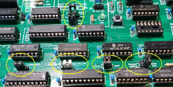
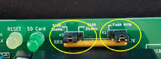
K5 |
S100 Enable / S100
Disable |
1-2 for Full Board
circuit in S100 bus. |
|
K1 |
Flash
Write |
2-3
Normally. 1-2 only if you want to program the Flash RAM (U3)
onboard. |
|
JP9 |
USB 5V |
Always open. |
|
JP2 |
Adaptor B |
Always open |
|
K10 |
Reset |
Jumper 2-3. This sets
the Z180 reset signal to come from the S100 bus
or the onboard switch SW1.
|
|
JP5 |
POC |
Jumpered, signal from
the s100 Bus. This should cause LED D4 to stay lit. |
| JP3 |
Slave Reset |
Jumpered, signal from
the S100 bus. |
|
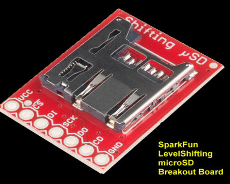
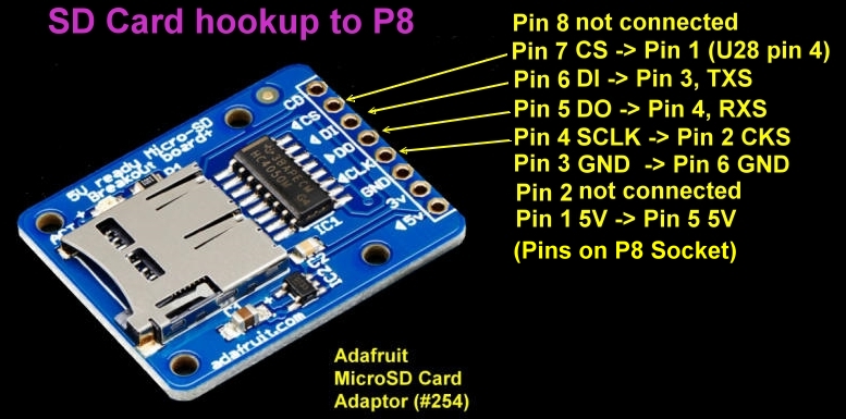
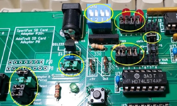
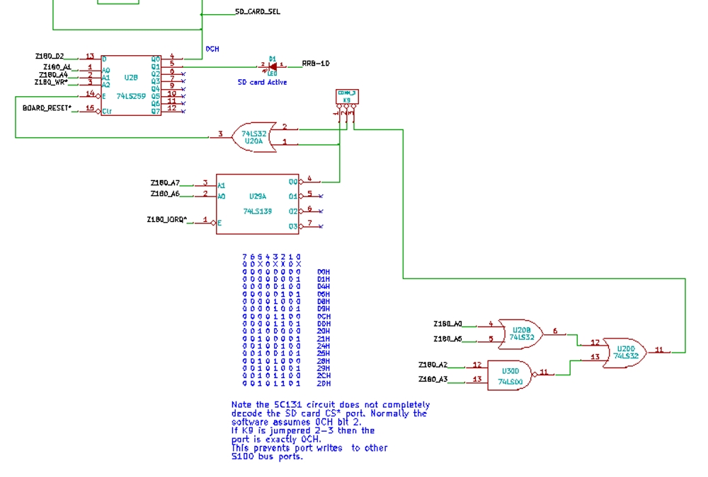
K9 |
SD Card port |
Defines the SD card
data port configuration. Jumper 2-3 (for exactly port 0CH) |
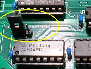
| K7 |
S100 or External Power |
2-3 for board from the
S100 bus. (Note pin 1 is on the right hand side) |
| K3 |
Non-IEEE |
Normally 2-3 |
| K8 |
Port 64 or 74 |
The IOBYTE port. Normally 2-3
(Port 75H) |
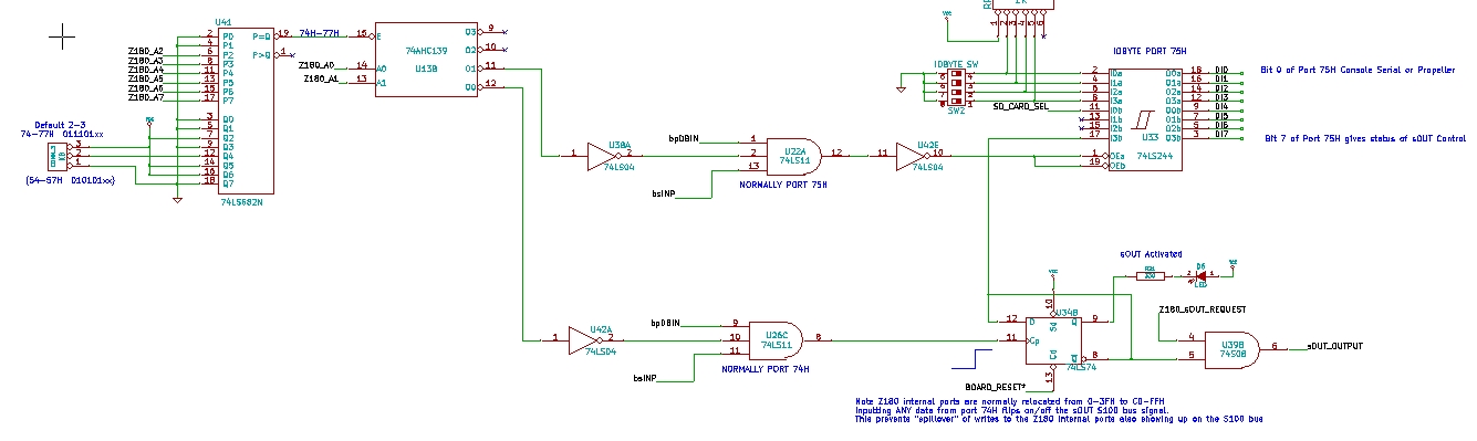
| P9 |
S100 signals |
Jumper Clock and MWRT.
Both vertical jumpers. |
| P3 |
S100 pSync |
Normally "pSYNC RAW".
Right most vertical jumper. |
| K2 |
PWFAIL/NMI |
Normally either none
or 2-3 (NMI) |
| JP7, JP6, JP8 |
IEEE-696 Ground |
Not normally required.
(Use to ground S100 signals 20, 53,70 in a fully IEEE-696 S100 bus
compliant system) |
| P4 |
IO Wait States |
0 to 8 IO wait states
can be added to the S100 bus to "stretch" the length of the fast
Z100 port Read/write signal.
Experiment, lower is better, typically
0-4 states depending on your S100 boards.
Jumper P4 1-2, 2-3, 4-5 & 6-7 for 4 wait states. |
| P5 |
sINTA,M1 or MEM Wait states |
1-2 to add an
interrupt acknowledge wait state. 2-3 for a Z80 "M1" memory read
wait states. 4-5 for all memory wait states. |
| P1 |
Wait States |
As for P4 this
determines the actual number of wait states requested by P5 |
| P15 |
Select Interrupt Vectors |
These select whether
the board handles incoming S100 interrupt signals VI0-VI7. (Not
currently used) |

.jpg)
.jpg)
.jpg)
.jpg)